State-of-the-art facility accelerates prototyping and commercialization
of miniaturized electronics products

TORONTO, July 2, 2014 /CNW/ - Celestica Inc. (NYSE, TSX: CLS), a global
leader in the delivery of end-to-end product lifecycle solutions, today
announced the opening of its new microelectronics laboratory at its
headquarters in Toronto, Ontario in Canada. The new facility will
enable start-ups, small and medium enterprises (SMEs) and large
original equipment manufacturers (OEMs) to quickly commercialize their
latest ideas for miniaturizing electronics products through prototyping
to volume production.
"Microelectronics is in demand for high-reliability markets such as
healthcare, aerospace, defense, communications and renewable energy. As
optics and photonics technologies permeate these high-reliability
sectors, it is becoming increasingly more important to miniaturize and
cost reduce," said Shawn Blakney, Senior Director, Technology and
Innovation, Celestica. "Smaller electronics provide the flexibility for
lighter, portable and potentially more affordable devices, a trend that
is already proven in the consumer market."
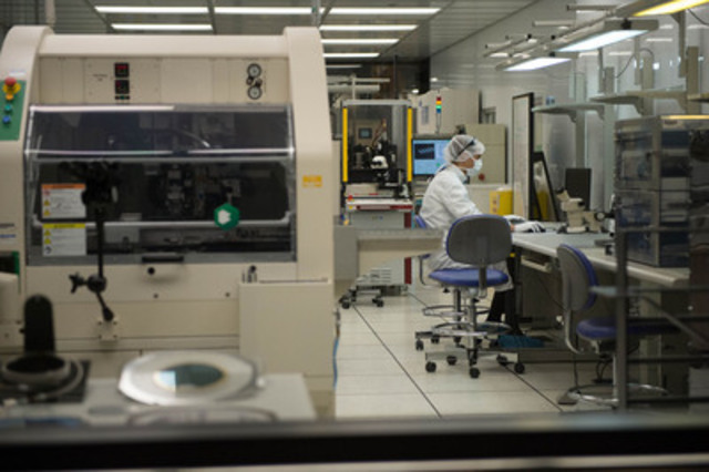
The unique 1100-square foot, ISO class-6 clean room is a controlled
environment for temperature, humidity and airborne particles. The
laboratory provides new miniaturization solutions using bare die
packaging technologies. The goal is to reduce production costs, enhance
signal integrity, and improve thermal performance for high-reliability
applications.
The location of the laboratory is a strategic choice with Toronto being
the largest ICT (Information, Communication and Technology) hub in
Canada. The laboratory will significantly bolster the infrastructure
for product enablement in Canada and may also be leveraged by global
customers looking to commercialize a product. Start ups, SMEs as well
as OEMs can now have quick access to talent and the technologies in
this facility to bring electronics products to target markets quickly
and affordably.
"The new microelectronics laboratory complements our existing
capabilities in Toronto including our materials laboratory and surface
mount technology manufacturing," added Blakney. "As we look to the
future, microelectronics will play an increasing role in technology,
and with this new capability, we can help our customers to keep up with
the pace of change and stay competitive in their markets."
About Celestica
Celestica is dedicated to delivering end-to-end product lifecycle
solutions to drive our customers' success. Through our simplified
global operations network and information technology platform, we are
solid partners who deliver informed, flexible solutions that enable our
customers to succeed in the markets they serve. Committed to providing
a truly differentiated customer experience, our agile and adaptive
employees share a proud history of demonstrated expertise and
creativity that provides our customers with the ability to overcome
complex challenges.
For further information on Celestica, visit its website at http://www.celestica.com.
The company's security filings can also be accessed at http://www.sedar.com and http://www.sec.gov.
Safe Harbour and Fair Disclosure Statement
Statements contained in this news release that are not historical facts
are forward-looking statements. Such forward-looking statements are
predictive in nature and may be based on current expectations,
forecasts or assumptions involving risks and uncertainties that could
cause actual outcomes to differ materially from the forward-looking
statements themselves. For those statements, we claim the protection of
the safe harbour for forward-looking statements contained in the U.S.
Private Securities Litigation Reform Act of 1995, and in applicable
Canadian securities legislation. Forward-looking statements are not
guarantees of future actions, events or outcomes. You should understand
that the risks, uncertainties and factors which are identified in our
various public filings at www.sedar.com and www.sec.gov could affect our future actions, events and outcomes and could cause
them to differ materially from those expressed in such forward-looking
statements. Forward-looking statements are provided for the purpose of
providing information about management's current expectations and plans
relating to the future. Readers are cautioned that such information
may not be appropriate for other purposes. Except as required by
applicable law, we disclaim any intention or obligation to update or
revise any forward-looking statements, whether as a result of new
information, future events or otherwise.
SOURCE Celestica Inc.
Image with caption: "Celestica's microelectronics lab in Toronto accelerates prototyping and commercialization of electronics products (CNW Group/Celestica Inc.)". Image available at: http://photos.newswire.ca/images/download/20140702_C9367_PHOTO_EN_41821.jpg
